ArF photoresist technology has high technical barriers and the global market is monopolized by Japanese companies

ArF photoresist is a type of semiconductor photoresist. It is a high-end photoresist product and is used to manufacture 12-inch large silicon wafers (silicon wafers). Among photoresist products, semiconductor photoresist has the highest technical barrier; among semiconductor photoresist products, ArF photoresist is one of the products with the highest technical content. ArF photoresist is the fourth generation photoresist. The technical barriers to entry in the industry are high and the number of global mass production companies is small.
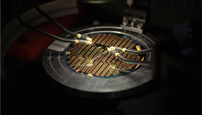
Globally, large-size silicon wafers have become a development trend. This is because the larger the diameter of a single silicon wafer, the greater the number of chips that can be manufactured and the lower the chip cost. At present, the global application proportion of large-size silicon wafers exceeds 94%, of which the application proportion of 12-inch large silicon wafers reaches 70%. ArF photoresist and EUV photoresist can be used to manufacture 12-inch large silicon wafers. EUV photoresist is currently the most advanced semiconductor photoresist, but EUV photoresist has higher technical barriers and its current production and sales are small. ArF photoresist is a mainstream product.
Semiconductor photoresist is the core material for chip manufacturing. Photoresist accounts for about 4% of the total cost of chip manufacturing materials. In the chip manufacturing process, the role of the photolithography process is to process fine circuit patterns. The resolution of the photoresist can directly affect the minimum feature size of the chip, and shortening the exposure wavelength can improve the resolution of the photoresist. As chip functional integration increases and process technology advances, the market demand for photoresists with shorter exposure wavelengths becomes stronger. ArF photoresist can achieve 193nm wavelength exposure and manufacture 7nm process technology chips. At present, 7nm chips have become the mainstream product in the market, so ArF photoresist is in high demand.
According to the “Comprehensive Research on the Market Status and Investment Prospects Forecast Report of China’s ArF Photoresist Industry from 2022 to 2026” released by the Industrial Research Center It shows that in 2021, in the global semiconductor photoresist market, ArF photoresist will account for 45%, the largest proportion, and is currently the most important semiconductor photoresist product. The global wafer industry is shifting to mainland China, China’s wafer production capacity continues to expand, and the scale of the semiconductor photoresist market continues to expand rapidly. In 2021, China’s semiconductor photoresist market will reach 2.92 billion yuan. At present, my country’s production strength in 12-inch large silicon wafers and 7nm chips is weak, and its demand mainly relies on imports. However, it is accelerating to catch up, and the demand for ArF photoresist is expected to continue to grow in the future.
The technical barriers to semiconductor photoresist are high, and my country’s market demand mainly relies on imports. Among the photoresist products produced by local companies in my country, PCB photoresist production with low technical content accounts for the largest proportion, while semiconductor photoresist production accounts for only about 2%. ArF photoresist is a high-end semiconductor photoresist. my country does not yet have large-scale mass production capabilities, and its demand basically relies on imports. In the global ArF photoresist market, Japanese companies are in a monopoly position. Five companies, JSR, Shin-Etsu, Tokyo Onka, Sumitomo, and Fuji, occupy 90% of the market share.
Industry analysts said that in the context of the information age, my country’s semiconductor industry is developing rapidly. In order to prevent key equipment, materials, and technologies from being The Chinese government has given strong support to the development of related enterprises. In the “Very Large Scale Integrated Circuit Manufacturing Equipment and Complete Set of Processes” project launched by the Chinese government, ArF photoresist is included, and companies such as Nanda Optoelectronics, Beijing Kehua, and Shanghai Xinyang undertake this research and development task. At present, Nanda Optoelectronics has independently developed ArF photoresist, obtained customer certification, and signed its first small batch order in September 2021. In the future, my country’s independent supply capacity of ArF photoresist is expected to gradually increase.

 微信扫一扫打赏
